By Daniel Oberhaus,’15 BA
Arizona is undergoing a major economic shift driven by the rapid expansion of its semiconductor sector, a transformation rooted in long-term planning and academic-industry collaboration led by Arizona State University (ASU). This growth did not occur spontaneously but through deliberate investments in education, infrastructure, and research capabilities. Sally C. Morton, who oversees research at ASU, described the current momentum as the outcome of sustained efforts that will continue benefiting the state for decades. She emphasized that the nation now relies on Arizona’s success in this high-stakes technological domain.
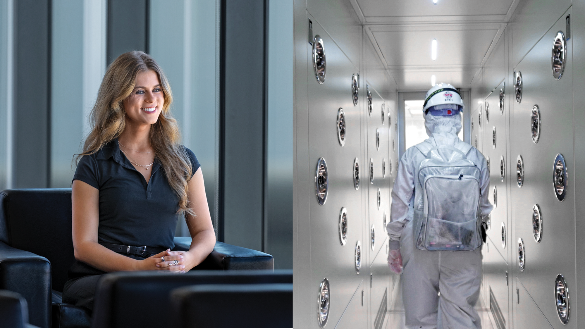
The semiconductor surge has drawn over $200 billion in private investment to the state in the past five years, according to the Arizona Commerce Authority. Major firms such as TSMC, Applied Materials, and Intel have established or expanded operations, generating thousands of high-skilled jobs. TSMC’s initial $12 billion commitment in 2020 grew into a $165 billion plan for six fabrication plants and two advanced packaging facilities—marking the largest foreign direct investment in U.S. history. Its first Arizona fab began producing 4nm chips this year, the most advanced chips ever made domestically, with future facilities set to manufacture even more sophisticated 2nm versions.
ASU has played a pivotal role by aligning its academic programs with industry demands. The university produces more than 7,400 engineering graduates annually, supplying a skilled workforce essential for semiconductor firms. Zak Holman, vice dean for research and innovation at ASU’s Ira A. Fulton Schools of Engineering, noted that partnerships with companies like Applied Materials were strategically designed to foster innovation. In 2023, Applied Materials invested $270 million to establish a Materials-to-Fab Center at ASU’s Research Park in Tempe, supported by ASU and the ACA. This facility hosts cutting-edge equipment for developing next-generation AI and microelectronics components.
The 2013 ACA investment in MacroTechnology Works laid the foundation for wafer-level packaging R&D and workforce training. Today, more than a dozen companies—from startups to global tech leaders—operate at the Tempe research park, contributing an additional $500 million in capital and collaborative research. This ecosystem has attracted federal support as well: in January, the U.S. Commerce Department selected Arizona for the NSTC Prototyping and NAPMP Advanced Packaging Piloting Facility, which will house unique semiconductor manufacturing and packaging technologies critical for national security and global competitiveness.
ASU President Michael M. Crow compared the significance of this development to the national laboratory expansions following the Manhattan Project, calling it one of the most substantial investments in U.S. research infrastructure in history. The vision dates back over a decade, when ASU, the Greater Phoenix Economic Council (GPEC), and ACA identified semiconductors as central to Arizona’s economic future. Chris Camacho, outgoing CEO of GPEC, credited ASU’s engineering talent pipeline as a decisive factor in attracting TSMC. With thousands of annual graduates in mechanical and electrical engineering, Arizona could demonstrate a viable workforce base for large-scale chip manufacturing.
The ripple effects extend beyond tech. For every semiconductor job created, an estimated five additional positions emerge in supporting sectors such as construction, food services, and childcare. Companies like Saras Micro Devices relocated to Chandler in 2023 to tap into the regional ecosystem. CEO Ron Huemoeller cited access to talent and proximity to industry partners as key reasons for the move. The firm, now employing 52 people with over 30 based in Arizona, expects its workforce to double by 2026, largely drawing from ASU graduates.
Economic spillovers are already visible. Lee Chi Investment Group, a real estate and food distribution company, acquired a partially occupied shopping center near TSMC’s site in 2024. Julia Li, operations director, noted increased tenant interest due to the anticipated influx of workers, reversing previous leasing challenges.
ASU continues refining its curriculum in collaboration with industry leaders to ensure students gain relevant skills. Katie Smith, a business development manager at ASU Knowledge Enterprise, stressed the importance of aligning education with workforce needs. Graduate Taylor Gowdy, hired by TSMC as an equipment engineer, highlighted the hands-on training at ASU’s Polytechnic campus as instrumental in securing employment.
Camacho described this era as one where chips become foundational to nearly every technology sector, offering Arizona a more stable and forward-looking economic base. With over $200 billion in semiconductor-related investment and a growing network of suppliers, manufacturers, and innovators, the state is positioning itself as a central hub in America’s tech resurgence.
— news from ASU News
— News Original —
How the semiconductor boom and ASU are transforming Arizona’s economy
By Daniel Oberhaus,’15 BA n nThe scale of the semiconductor industry’s economic impact in Phoenix is unprecedented — but it isn’t happening by accident. It’s the result of years of effort led by ASU, which has created the largest engineering school in the U.S. and developed the state-of-the-art facilities that are fueling the semiconductor boom and countless technological breakthroughs in the industry. n n“What is happening in Arizona is the culmination of the work of many people over many years, and it will benefit the state for many years to come. It is a reason to celebrate where we have come from, where we are and what we are becoming — and the nation is depending on us to succeed,” explains Sally C. Morton, who leads research at ASU. n nThis coordinated effort has attracted tens of billions of dollars in new investment to Arizona from companies, including Applied Materials, TSMC and dozens of other semiconductor companies, creating thousands of additional high-tech jobs. n nAs a result, the semiconductor industry’s growth in Arizona is paving the way for hundreds of new small businesses, ranging from parts suppliers to restaurants. Dozens of new ASU workforce development programs and major public works projects will also improve roads, water facilities and other infrastructure across the Valley. n nThe key to attracting the world’s top semiconductor companies to the Valley was creating pathways for them to collaborate with world-class researchers at ASU, says Zak Holman, the vice dean for research and innovation at ASU’s Ira A. Fulton Schools of Engineering. For more than a decade, Holman has helped shape ASU’s semiconductor strategy by forging partnerships with industry. n n“Partnering with Applied Materials, which is the world’s leading semiconductor equipment manufacturer, was a very purposeful choice,” Holman says. “We needed to bring in unique equipment to ASU, and Applied Materials needed innovative people developing unique things on their equipment so they could sell it to their customers like Intel or TSMC.” n nASU’s industry partnerships are working. In July 2023, Applied Materials announced a $270 million investment to create a Materials-to-Fab Center at ASU’s Research Park in Tempe, which ASU and the Arizona Commerce Authority contributed to as well. This investment includes installing machines at ASU’s MacroTechnology Works that make materials for the next generation of AI and microelectronics chips. n nThe multimillion-dollar investment that ACA made in 2013 to MacroTechnology Works will enhance Arizona’s wafer-level packaging R&D and workforce training capabilities for Arizona. n nAll told, more than a dozen companies, ranging from local startups to multinational tech giants, have taken up residence at the park in Tempe and invested an additional $500 million in the facility and sponsored research agreements with ASU. This center of gravity has attracted still more microelectronics companies, as well as additional funding including government research programs. n nIn January, the U.S. Commerce Department announced that the new NSTC Prototyping and NAPMP Advanced Packaging Piloting Facility would be located in Arizona, adjacent to the MacroTechnology Works building. This facility will be home to bleeding-edge semiconductor prototyping, manufacturing and packaging equipment that isn’t available anywhere else in the world, creating a domestic R&D capability that is vital for America’s national security and maintaining its position as a global leader in semiconductor innovation. n nASU President Michael M. Crow put the state’s win in context, saying, “This is the largest of three CHIPS R&D flagship facilities being launched that together represent the greatest national laboratory investments since those that came out of the Manhattan Project.” n nTen years ago and even before, ASU and other entities such as the Greater Phoenix Economic Council and ACA were already looking to semiconductors as Arizona’s future. n nCrow, other leaders at ASU and GPEC understood that chips are required for everything. n nToday, virtually all computer chips are made abroad and depend on a global supply chain that is increasingly dominated by China. Although the U.S. does produce some computer chips domestically, the vast majority of the chips in our phones, computers and other electronics are made by TSMC in Taiwan. n nAbout a decade ago, ASU, the ACA and other organizations, including GPEC, launched a campaign to bring TSMC’s first fab in the U.S. to Phoenix. From GPEC’s perspective, what really sealed the deal was the workforce and research depth at ASU. n n“ASU has thousands of graduates per year in mechanical and electrical engineering, which meant we could illustrate to TSMC that this was the market they should launch and scale from in the United States,” says Chris Camacho, outgoing president and CEO of GPEC. n nIn 2020, TSMC committed $12 billion to build a fab in Arizona, then expanded that to $165 billion for six fabs and two advanced packaging facilities. It’s the largest foreign direct investment in U.S. history. n nAs of this year, its first fab has started producing advanced 4nm chips for U.S. customers — the first time these types of chips have ever been produced on U.S. soil. The company’s second and third fabrication plants are currently under construction and when complete will produce 2nm chips, which are the most advanced commercially available chips in the world. n nAccording to GPEC’s analysis, TSMC’s first three fabs alone will create 6,000 jobs and more than $33 billion in direct and indirect economic output for the people of Arizona. GPEC also estimates that for every job created in the semiconductor industry, it will also create five new jobs in other industries that support this new workforce, such as construction, restaurants and child care. n nThe semiconductor industry depends on a vast network of interconnected suppliers. Arizona is unique in the U.S. because it has all elements of the semiconductor supply chain, which benefit both large companies, as well as semiconductor companies like Saras Micro Devices. n nWhen Ron Huemoeller was tapped to lead Saras Micro Devices as its new CEO in 2023, one of his first major initiatives was finding a new home for the company because it was hard to find enough talent in Atlanta. So last year Huemoeller relocated the company to Chandler to benefit both from the proximity to other semiconductor companies and ASU. n n“The primary driver to establish the headquarters in Arizona was because of the broad semiconductor ecosystem that is growing here,” says Huemoeller. n nThe company now employs 52 people, and more than 30 of them work in Chandler. Huemoeller says he expects the company’s head count to double by the end of 2026, with many new hires coming from ASU. n n“We feel comfortable that we will be able to access the right people for our company here,” he says. n nThe semiconductor boom’s economic benefits extend far beyond tech manufacturing. This trend is already visible across the Valley, from construction companies working on fab builds to restaurants opening. n nOne of the dozens of examples is Lee Chi Investment Group, a large food distributor and a local real estate investor. In 2024, Lee Chi acquired a shopping center in north Phoenix about 20 minutes from TSMC. At the time, the shopping center was only about 75% occupied but, with TSMC so close, is now growing. n n“At this location, people are coming to us because they see the opportunity; usually we have the opposite problem,” says Julia Li, director of operations for the group. n nASU’s engineering program graduates more than 7,400 students a year. These graduates are essential to the semiconductor companies’ success. n n“Companies like Intel and TSMC need an excellent, well-trained workforce and a lot of people,” Holman says. “ASU has both the volume and quality of graduates to meet that need.” n nOne of those graduates is Taylor Gowdy, ’24 BSE in engineering (mechanical engineering systems), who was hired by TSMC in 2024 as an equipment engineer. She attended classes on ASU’s Polytechnic campus, which provided a hands-on, project-based emphasis. n n“There are so many engineering opportunities here,” Gowdy says. “So if someone is looking to work in manufacturing, there will be a role that fulfills their interests.” n nASU has been working closely with Applied Materials, TSMC, Intel and dozens of other companies to understand their needs and tailor programs so that students develop the skills to land a job in the industry when they graduate. n n“We work really hard to collaborate with our corporate partners to understand the workforce and build the curriculum to fill those gaps,” says Katie Smith, ’13 BS in biochemistry, ’17 MBA, a business development manager at ASU Knowledge Enterprise who leads microelectronics engagements. n nFor Phoenix, and Arizona more broadly, semiconductors represent more than just another industry. The semiconductor industry offers a sixth C — “chips” — that will be less cyclical and more future-proof. n n“We’re entering a new era where chips are going to be the center of everything,” Camacho says. “Our economy is now going to be anchored to products that are integrated in the most sophisticated way into virtually every channel of technology.” n nThe numbers support this optimism. According to the Arizona Commerce Authority, in the last five years, there has been more than $200 billion in private investment in Arizona related to semiconductors. n n“My children and my children’s children will look back at all the semiconductor growth that’s happening now and see that it was a pivotal point for Arizona’s economy,” Camacho says.